INDRBT / Reading room
Understand the joint-interface components
Adapted for browser reading from the project’s illustrated documentation. Numeric results and engineering scope are unchanged. Reproduction notes are optional; the robot and board viewers run from the navigation above.
On this page
Start with the schematic PDF, then locate the same reference on the PCB top view. A reference such as R5 identifies one component across the schematic, BOM and PCB. R means resistor, C capacitor, D diode/LED, U integrated circuit, J connector, F fuse and JP jumper.
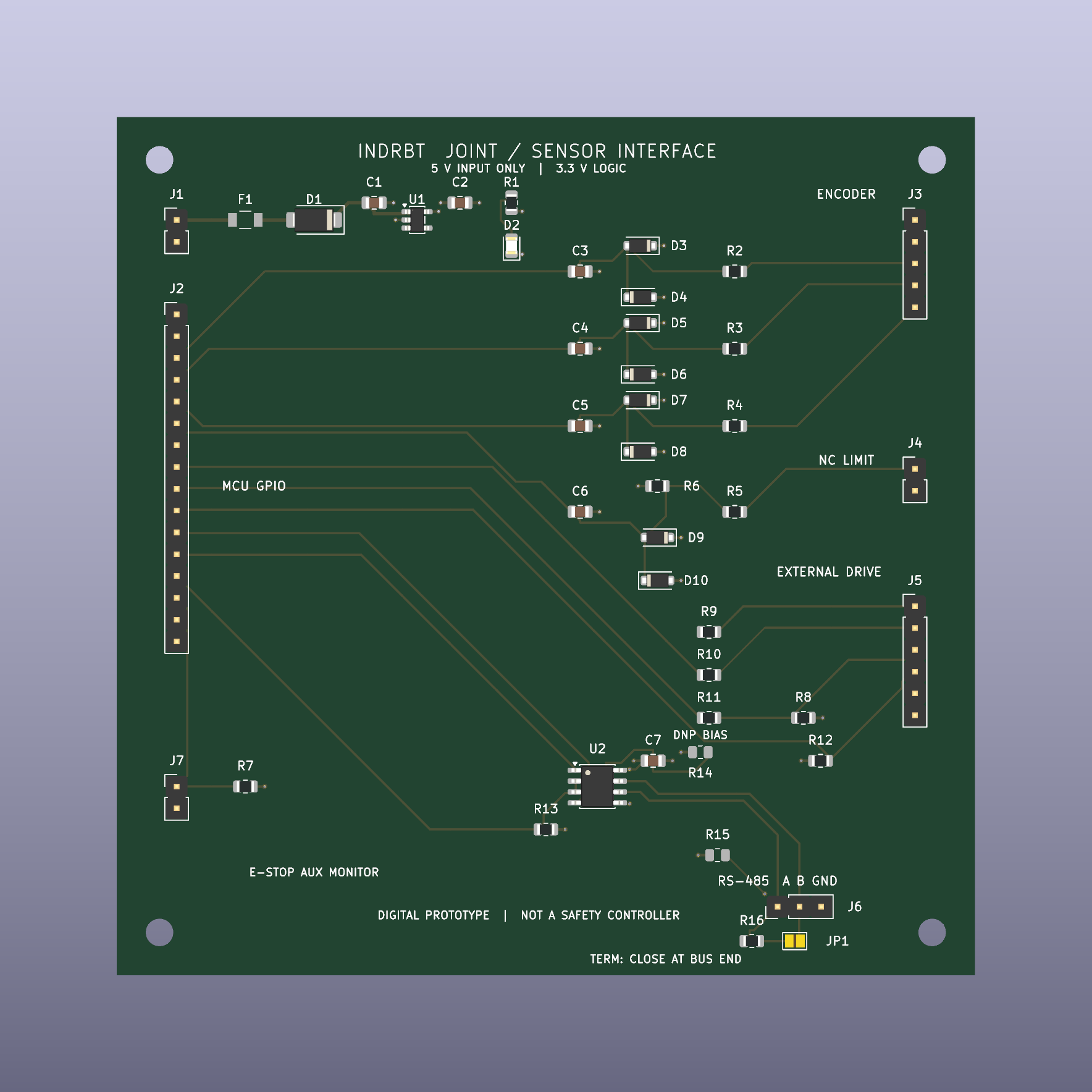
The BOM CSV is the detailed component list. Fit means included in the default design. DNP means “do not populate”: the pads exist, but the component is omitted. This is a checked digital interface for an external controller and motor drive. It is not a complete motor controller or a qualified purchase order.
| References | Role and selected value | What the selection means |
|---|---|---|
| J1, F1, D1 | 5 V input, resettable fuse, reverse-polarity diode | F1 is Bourns MF-NSMF025X-2, with a project-local manufacturer land pattern. D1 is the SS14 SMA family. Supply only regulated 5 V; there is no overvoltage limiter. |
| U1, C1, C2 | AP2112K-3.3 regulator; 10 µF input and 4.7 µF output capacitors | SOT-23-5/SOT25 pinout. Use 10 V rated X7R/X5R 0805 ceramics, checking their effective capacitance under DC bias; at least 1 µF must remain on the output. The 150 mA shared budget is a design target. |
| R1, D2 | 1 kΩ and green 0805 LED | Shows that the 3.3 V rail is present. LED polarity matters; brightness and forward voltage depend on the exact LED selected. It does not indicate firmware or motor status. |
| J2, J3; R2–R4, C3–C5, D3–D8 | Controller and encoder headers; 1 kΩ/100 pF filters and BAT54H clamps | Three quadrature channels A/B/Z. Select C0G/NP0 100 pF 0805 capacitors. Clamps reduce modest excursions; they do not establish industrial ESD protection or 5 V compatibility. |
| J4; R5, R6, C6, D9, D10 | Normally closed limit contact; 1 kΩ, 10 kΩ and 100 nF filter | Closed contact gives a low signal. An open contact or broken wire gives a high signal. External controller inputs need Schmitt hysteresis and firmware debounce. A short to ground can defeat fault detection. |
| J7, R7 | Normally closed E-stop auxiliary monitor; 10 kΩ pull-up | Reports contact state only. Actual torque interruption belongs to external safety hardware. |
| J5; R8–R12 | External-drive commands, fault input and pull resistors | 330 Ω series resistors on STEP/DIR/ENABLE; 10 kΩ pull-down on ENABLE and pull-up on FAULT. The selected drive must accept 3.3 V signals and the documented polarity. |
| U2, C7, R13, J6 | LTC2850IS8 RS-485 transceiver, 100 nF bypass and 10 kΩ direction pull-down | SOIC-8, 1.27 mm pitch. Default direction is receive. 250 kbit/s is the system target; protocol and embedded firmware are not implemented on this board. |
| R14, R15 | Optional 330 Ω bus bias; DNP by default | U2 includes receiver failsafe. If an installation requires external bias, fit the pair at exactly one node and evaluate cable/common-mode effects. |
| R16, JP1 | 120 Ω bus-end termination and open solder jumper | Close JP1 only at the two physical cable endpoints. Specify a 1% 0805 resistor rated at least 0.25 W, with temperature derating reviewed. Its conservative 3.3 V differential power bound is about 91 mW. JP1 is bare copper, so it has no placement-file body. |
| H1–H4 | Four 3.2 mm nonplated mounting holes | Board-only mechanical features, excluded from the BOM and placement file. |
Use 1% 0805 resistors for the network values; physical resistor power/temperature ratings and exact ordering codes still require selection. C6/C7 may use X7R 100 nF 50 V 0805 parts. The regulator's heat estimate includes both the voltage drop carrying the load and its own quiescent supply current; even an unloaded regulator consumes power. This remains a reference calculation, with physical temperature and component tolerance limits open. The headers are generic 2.54 mm single-row connections for a student prototype; keyed enclosure connectors, retention and cable assemblies would need a separate physical design review.
The stock SMA, SOD-123F, SOT-23-5 and SOIC-8 footprints agree with the specified package families and pin counts. Generic library pads can differ from a manufacturer's suggested soldering pattern; only F1's copper pads are deliberately transcribed and dimension-checked against its manufacturer's nominal drawing. No complete assembly-process qualification is claimed. The local F1 file includes copper, paste, mask, fabrication and courtyard geometry; it has no manufacturer-specific 3D body model, so the rendered picture shows its lands rather than a fitted fuse body.
Read the electrical design chapter for pin contracts, calculations, rule scope and reproduction. Primary component sources are the Bourns fuse, AP2112 regulator, SS14 diode family, BAT54H clamps, and LTC2850 transceiver.
To inspect the saved evidence without KiCad, run python electronics/review_electronics.py from the source directory. This recomputes hashes and checks BOM/board agreement, placement population, fabrication package contents and drill counts. A fresh native ERC/DRC run still requires python electronics/run_checks.py with KiCad installed.